チップパッケージフィルムの進化: 保護からパフォーマンス向上まで
Chip Packaged Filメートル
In the fast-paced world of semiconductor technology and snack food innovation, Chip Packaged Film has emerged as a critical component that bridges functionality, 保護, そして消費者の経験. デリケートなマイクロチップを保護するか、ポテトチップスのパリパリ感を保持するかどうか, この専門の映画技術は、現代産業の要求を満たすために進化しています. Let’s explore how Chip Packaged Film is reshaping packaging across two vastly different yet interconnected sectors.
1. Semiconductor Industry: The High-Tech Shield
In electronics, Chip Packaged Film refers to advanced materials and techniques used to encase semiconductor devices, ensuring their performance, 耐久性, and thermal management. As chips become smaller, もっと早く, and more complex, packaging films must adapt to support these innovations.
Key Trends:
- 3D & 2.5D Stacking: Modern films enable multi-layer chip stacking, reducing footprint while improving signal integrity. 例えば, System-in-Package (SiP) solutions integrate logic, memory, and RF components into a single compact unit, relying on high-precision films for electrical insulation and heat dissipation.
- Fan-Out Wafer-Level Packaging (FOWLP): This technique distributes interconnects across a larger area, enhancing thermal performance. Films here act as a protective layer, shielding chips from physical stress and environmental factors like moisture.
- 持続可能性: Leading manufacturers are adopting eco-friendly films, such as biodegradable polymers or recycled materials, to reduce carbon footprints. 例えば, some companies are exploring carbon-neutral packaging processes aligned with global sustainability goals.
Market Impact:
The semiconductor packaging market is projected to grow from30.76バイll私ああの2023tああ45 10億 2035, driven by AI, 5G, and electric vehicles. Innovations in film technology, のようにflip-chip bonding そしてadvanced underfill materials, are key contributors to this expansion.
2. Snack Food Industry: Freshness Meets Functionality
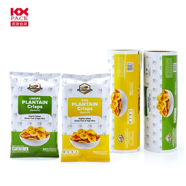
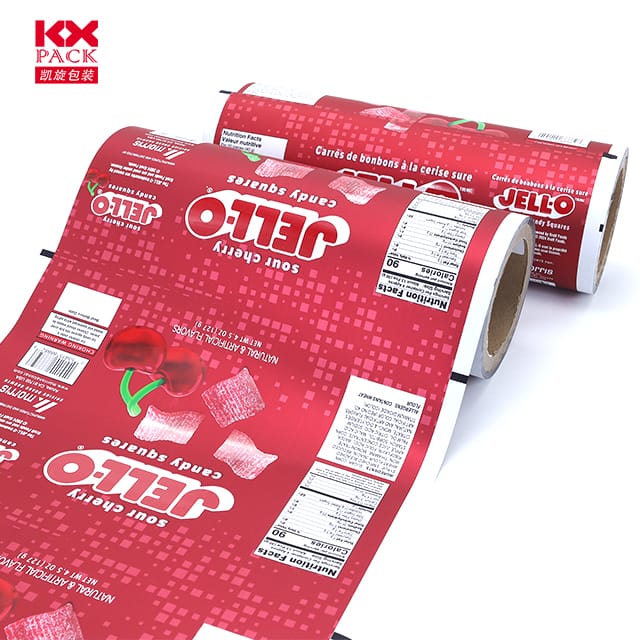
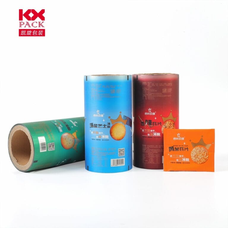
For potato chips, ナッツ, and other snacks, Chip Packaged Film is a multi-layered barrier designed to preserve taste, テクスチャー, and shelf life. This film must balance flexibility, 強さ, and barrier properties against oxygen, 水分, そして光.
主な特長:
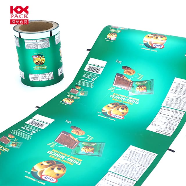
- High-Barrier Laminates: Modern snack films combine materials like ペット (ポリエステル), アルミホイル, とPE (ポリエチレン) to create impermeable layers. 例えば, a typical chip bag might use:
- Outer printing layer (ペット): For vibrant branding.
- Metalized or foil layer: Blocks oxygen and light.
- Inner sealant layer (PE/CPP): Ensures airtight closure.
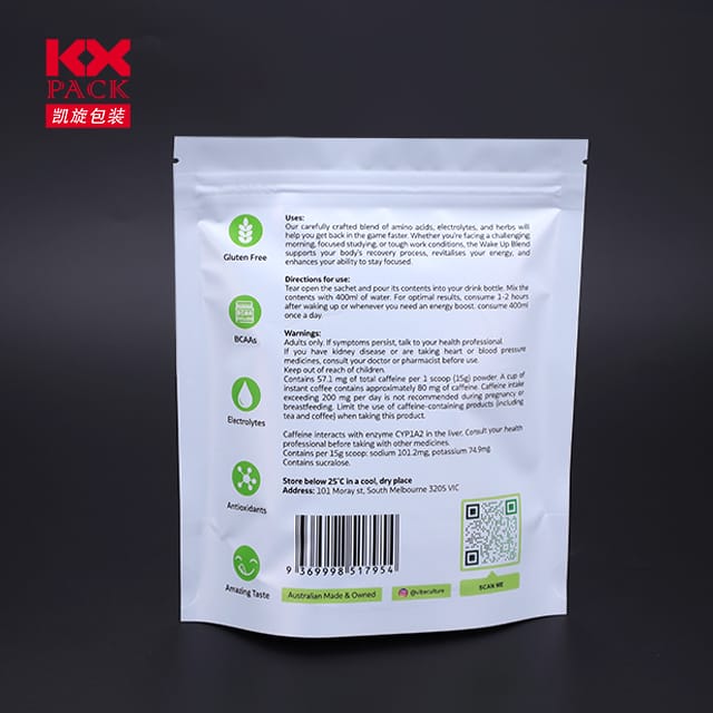
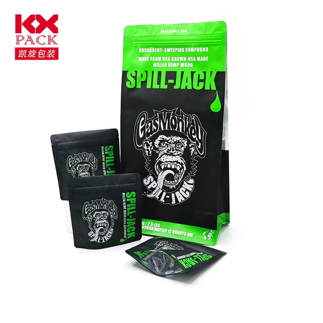
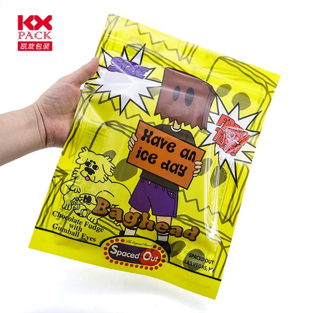
- Convenience Enhancements: Easy-open tabs, 再封可能なジッパー, and stand-up pouches are now standard, improving user experience and reducing food waste.
- Sustainability Shifts: Brands are transitioning to 堆肥化可能なフィルム (例えば。, 人民解放軍, PBS) or recycled content to appeal to eco-conscious consumers. Some companies report a 30% reduction in plastic use by optimizing film thickness without compromising performance.
Market Dynamics:
The global snack packaging market is booming, with innovations likehigh-speed automated packing machines そしてanti-fogging films (to prevent condensation inside bags) driving efficiency. Consumers now expect packaging that’s not just functional but also visually appealing—a trend fueled by social media and unboxing culture.
Cross-Industry Parallels: Innovation at the Core
Despite serving different markets, both semiconductor and snack industries share a common goal: pushing the boundaries of material science to deliver superior performance. 例えば:
- Miniaturization: Semiconductor films enable smaller, more powerful chips, while snack films allow for portion-controlled, on-the-go packaging.
- Thermal Management: In electronics, films dissipate heat; in snacks, they prevent sogginess by blocking humidity.
- カスタマイズ: Both sectors demand tailored solutions—whether it’s a film for a high-frequency 5G chip or a gluten-free snack pouch.
The Future of Chip Packaged Film
先を見ています, we can expect:
- スマート映画: Embedded sensors in semiconductor packaging could monitor chip health in real time, while snack films might use 時間温度インジケーター to ensure freshness.
- Hybrid Materials: Combining organic and inorganic layers to create films that are both conductive and biodegradable.
- 循環経済の統合: More brands will adopt reusable or recyclable films, aligning with global zero-waste targets.
結論
Chip Packaged Film is far more than a protective layer—it’s a catalyst for innovation. In electronics, it enables the next generation of AI and IoT devices; in snacks, it redefines convenience and sustainability. As industries continue to evolve, so too will the films that support them, proving that even the smallest components can drive massive change.
Whether you’re munching on chips or scrolling through a smartphone, take a moment to appreciate the unsung hero: the packaging film that makes it all possible. 🌍✨

